
 The U.S. Department of Commerce has identified advanced materials as one of five emerging technologies the United States must master to remain competitive in the world marketplace. The Department of Materials Science and Engineering addresses the educational and technological challenges of creating, applying, and characterizing new materials for manufacturing products for the 21st century.
The MTSE department has facilities to study:
- Properties of polymers and composites, including thermophysical, rheological, and mechanical properties of solids, liquid crystals, melts and solutions
- Surface analytical chemistry, including metal-polymer interfaces, adhesion, corrosion, and chemical vapor deposition
- Scanning of electron microscopy and Auger spectroscopy of magnetic materials
- Optical, magnetic, and electrical characterization and analysis
- Scanning of tunneling microscopy; resonant ionization mass spectrometry
- Solderability and X-ray diffraction
- Low-energy electron diffraction
- Electrical characterization
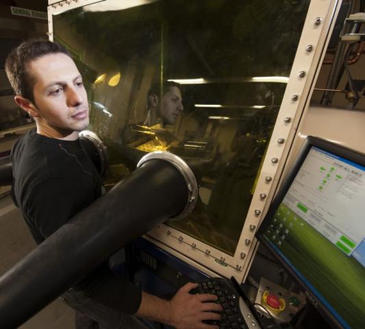
MTSE research facilities
Departmental Major Shared Equipment
The MTSE department has undergone much expansion in the past couple years, primarily as a result of congressional and Department of Defense/Army Research Laboratory support. Part of this expansion included the acquisition of new state-of-the-art major equipment that allows our students and faculty to perform advanced research and studies.
Students in the Department of Materials Science and Engineering also have access to other university equipment that is supervised by the Laboratory for Atomic Scale Characterization. For more information, visit the Materials Research Facility.
Laboratory for Electronic Materials and Devices (LEMD)
This new laboratory uses an ultrahigh vacuum cluster tool deposition system to combine surface science and ion beam characterization techniques with in-situ growth capability. Topics of investigation include advanced gate dielectrics and devices, high-field chemical reaction pathways and surface preparation for enhanced device performance.
Some of the techniques and skills supported by the LEMD include:
- X-ray Photoelectron and Auger Electron Spectography
- Scanning Tunneling Microscopy
- Atomic Force Microscopy
- Thermal Desorption Spectroscopy
- Rutherford Backscattering
- Ion Channeling
For more information, visit the Materials Research Facility.
Laboratory for Atomic Scale Characterization
The Laboratory for Atomic Scale Characterization houses equipment brought in under Advanced Resource Technologies, Inc. Available equipment includes:
- FEI Tecnai F20ST TEM
- FEI Nova 200 Analytical Dual Beam FIB
- Imago LEAP
- Philips EM420 TEM
- JOEL 5800 SEM
- Several optical microscopes for characterization of virtually any material
For more information, visit the Materials Research Facility.
Laboratory of Advanced Polymers and Optimized Materials (LAPOM)
This lab allows for the development of materials with improved mechanical, tribological and thermophysical properties, including thermoplastics, thermosets, polymer-based composites and coatings.
Properties tested by students and faculty in the LAPOM include:
- High strength
- Wide service temperature range
- Low thermal expansivity
- Low static and dynamic surface friction
- High adhesion of coatings to ceramic and metal substrates
- High scratch and mar resistance
For more information, visit LAPOM.
Materials Synthesis and Processing Laboratory
Research interests focus on the development and characterization of aerogels, xerogels, and other ovel ceramics for semiconductor, dielectric energy, and sensor applications. Low K xerogel films, biomaterial growth templates and antibacterial coatings are some of the current research programs being studied in the Materials Synthesis and Processing Laboratory.
Some of the characterization techniques students and faculty use in this lab include:
- Small angle neutron scattering
- Scanning/transmission electron microscopy
- Gas absorption
- Infrared spectroscopy
Energy Materials Laboratory
The Department of Materials Science and Engineering is currently researching several areas related to alternative energy production. Currently, the two primary areas of focus are:
- 3-D atomic scale characterization of electronic and optoelectronic nanostructures for photovoltaics (solar cells) and microelectronics using FIB, (S)TEM tomography, and laser pulsed local electrode atom probe (LEAP)
- Low-temperature, high-utilization, direct-write processing for solid oxide fuel cells and photovoltaic electrical contacts (metals and transparent conducting oxides)
Laboratory for Laser Materials Synthesis and Fabrication
The laboratory is involved in fundamental understanding of laser-material interactions. Such understanding is intended for utilization of high power lasers for the purposes such as surface engineering, coating, machining and synthesis of advanced metallic and ceramic materials. The laboratory houses the following laser systems.
- 3 kW Ytterbium (1.07 µm wavelength) fiber optic beam delivery laser system equipped with high frequency beam scanning head for large area coverage and 5-axis workpiece motion system for additive manufacturing, advanced machining and surface engineering.
- 1 kW Nd-Yag ((1.06 µm wavelength) multiplex (dual fiber) fiber optic beam delivery system equipped with two independent multiaxis workpiece motion system for manufacturing, advanced machining and surface engineering.
- 400J pulsed Nd-Yag ((1.06 µm wavelength) fiber optic beam delivery system equipped with multiaxis workpiece motion system for manufacturing and surface engineering.
- Post laser manufacturing and processing characterization equipment: wear and friction tribometer, potentiostatic corrosion cell, contact angle measurement unit for wettability testing.
MTSE research equipment
Some of the instrumentation available through the UNT Center for Advanced Research and Technology and individual faculty labs are described below.
Imaging
- High-Resolution Analytical TE: FEI Tecnai G2 F20 S-Twin 200keV field emission scanning transmission electron microscope (S/TEM) with precession electron diffraction (PED)
- Dual Beam SEM/FIB: FEI Nova 200 NanoLab: a dual column ultra-high resolution field emission scanning electron microscope (SEM) and focused ion beam (FIB)
- High Resolution FEG SEM: FEI Nova NanoSEM 230
- Environmental SEM: FEI Quanta environmental scanning electron microscope (ESEM)
- 3-D Atom Probe: Cameca local electrode atom probe (LEAP) instrument with added laser-pulsed evaporation technique
- Atomic Force Microscope: Veeco (Digital Instruments) Multimode Nanoscope III
- X-Ray Tomography: X-Ray Tomography Skyscan 1172
Spectroscopy
- High Resolution X-ray Diffraction: Rigaku Ultima III high-resolution XRD with high temperature stage, small x-ray scattering, and in-plane measurement capability
- X-ray Photoelectron Spectrometer: PHI 5000 Versaprobe
- Scanning Auger Nanoprobe: PHI 670xi
- Fourier Transform Infrared Spectrometer and microscope: Thermo Electron Nicolet 6700 FTIR
- Spectroscopic Ellipsometers: J.A. Woollam variable angle spectroscopic ellipsometer (VASE) and J.A. Woollam M-2000
- Raman Spectrometer: Thermo Electron Almega XR
- IR Ellipsometer: JA Woollam Infrared Variable Angle Spectroscopic Ellipsometer
- Fourier Transform Infrared Spectrometer: Nicolet Nexus 470 FTIR with thin film grazing angle, ATR, liquid cell, variable angle, variable temperature capabilities, supercritical transmission cell
Material testing
- Instrumented Impact Tester: Instron Dynatup® 9250HV impact tester
- Hall Effect Measurement System: Ecopia HMS-5000
- Rheometer: TA Instruments ARES-LS2 rheometer
- Tribometer: Microphotonics pin-on-disk tribometer
- Profilometer: Veeco Dektak 150
- Impedance Analyzer: Solartron
- Thermomechanical analyzer: Perkin-Elmer Model TMA-7
- Differential scanning calorimeter: Perkin-Elmer Model DSC-7
- Thermogravimetric analyzer: Perkin-Elmer TGA-7
- Dynamic mechanical analyzer: Perkin-Elmer DMA-7
- Dynamic mechanical thermal analyzer: Rheometrics DMTA
- Computerized universal testing machine – SINTECH
- Rheometer: Rheometrics SR5
- Viscometer: Brookfield DV-II+ Programmable Viscometer
- C-V/I-V Measurement: Micromanipulator probe station + Agilent 4294A Impedance Analyzer, Agilent 4156B Parameter Analyzer with variable temperature
Processing
- OLED (organic light emitting device) Evaporator: Custom built deposition system for organic thin film applications
- Biopolymer Extruder: American Leistritz Extruder Corp extruder for film, sheet, and ribbon extrusion
- Laser Engineered Net Shaping: Optomec LENS 750
- Maskless Mesoscale Materials Deposition: Aerosol Jet Optomec Aerosol Jet deposition system
- Physical Vapor Deposition: Kurt J. Lesker PVD-75
- Etching and Coating System: Gatan PECS
- Laboratory Extruder: Randcastle
- Tape Caster: Mistler with 4” and 12” doctor blades
- Supercritical driers: Polaron 3000 and Samdri
- Supercritical reactor: made in house capable for 200mm Si wafers
- Photoresist spinner: Headway
- Atomic layer deposition (ALD) system
- UHV magnetron sputter deposition (PVD 75) system
- Laser processing: 400J Nd-YAG Pulse Lasers include: Lumonics JK701 400W, Rofin Sinar Starweld 250 3000 W, Ytterbium YAG (IPG3000)
- Friction stir welding